- 您现在的位置:买卖IC网 > Sheet目录337 > LT3597EUHG#PBF (Linear Technology)IC LED DRIVER TRPL STP DWN 52QFN
�� �
�
�LT3597�
�APPLICATIONS� INFORMATION�
�f� SW(MAX)� =�
�(� )�
�V� OUT(MAX)� =� 1.1� V� LED(MAX)� +� 1.1V� =� 1.2V� ?� ?� 1� +�
�?� R2� ?�
�?�
�R1� ?�
�Selecting the optimum switching frequency depends�
�on� several� factors.� Inductor� size� is� reduced� with� higher�
�frequency,� but� efficiency� drops� slightly� due� to� higher�
�switching� losses.� Some� applications� require� very� low�
�duty� cycles� to� drive� a� small� number� of� LEDs� from� a� high�
�supply.� Low� switching� frequency� allows� a� greater� range�
�of� operational� duty� cycle� and� hence� a� lower� number� of�
�LEDs� can� be� driven.� In� each� case,� the� switching� frequency�
�can� be� tailored� to� provide� the� optimum� solution.� When�
�programming� the� switching� frequency,� the� total� power�
�losses� within� the� IC� should� be� considered.�
�Switching� Frequency� Synchronization�
�The� nominal� operating� frequency� of� the� LT3597� is� pro-�
�grammed� using� a� resistor� from� the� RT� pin� to� ground�
�over� a� 200kHz� to� 1MHz� range.� In� addition,� the� internal�
�oscillator� can� be� synchronized� to� an� external� clock� applied�
�to� the� SYNC� pin.� The� synchronizing� clock� signal� input� to�
�the� LT3597� must� have� a� frequency� between� 240kHz� and�
�1MHz,� a� duty� cycle� between� 20%� and� 80%,� a� low� state�
�below� 0.4V� and� a� high� state� above� 1.6V.� Synchronization�
�signals� outside� of� these� parameters� will� cause� erratic�
�switching� behavior.� For� proper� operation,� an� R� T� resistor�
�is� chosen� to� program� a� switching� frequency� 20%� slower�
�than� the� SYNC� pulse� frequency.� Synchronization� occurs�
�at� a� fixed� delay� after� the� rising� edge� of� SYNC.�
�The� SYNC� pin� must� be� grounded� if� the� clock� synchroniza-�
�tion� feature� is� not� used.� When� the� SYNC� pin� is� grounded,�
�the� internal� oscillator� controls� the� switching� frequency� of�
�the� converter.�
�Operating� Frequency� Trade-offs�
�Selection� of� the� operating� frequency� is� a� trade-off� between�
�efficiency,� component� size,� output� voltage� and� maximum�
�input� voltage.� The� advantage� of� high� frequency� operation�
�is� smaller� component� sizes� and� values.� The� disadvantages�
�are� lower� efficiency� and� lower� input� voltage� range� for� a�
�desired� output� voltage.� The� highest� acceptable� switch-�
�ing� frequency� (f� SW(MAX)� )� for� a� given� application� can� be�
�calculated� as� follows:�
�V� D� +� V� OUT�
�t� ON(MIN)� (� V� D� +� V� IN� ?� V� SW� )�
�where� V� IN� is� the� typical� input� voltage,� V� OUT� is� the� output�
�voltage,� V� D� is� the� catch� diode� drop� (0.5V)� and� V� SW� is� the�
�internal� switch� drop� (0.5V� at� max� load).� This� equation�
�shows� that� slower� switching� is� necessary� to� accommodate�
�high� V� IN� /V� OUT� ratios.� The� reason� the� input� voltage� range�
�depends� on� the� switching� frequency� is� due� to� the� finite�
�minimum� switch� on� and� off� times.� The� switch� minimum�
�on� and� off� times� are� 200ns.�
�Adaptive� Loop� Control�
�The� LT3597� uses� an� adaptive� control� mechanism� to� set�
�the� buck� output� voltage.� This� control� scheme� ensures�
�maximum� efficiency� while� not� compromising� minimum�
�PWM� pulse� widths.� When� PWM1-3� is� low,� the� output� of�
�the� respective� buck� rises� to� a� maximum� value� set� by� an�
�external� resistor� divider� to� the� respective� FB� pin.� Once�
�PWM1-3� goes� high,� the� output� voltage� is� adaptively� re-�
�duced� until� the� voltage� across� the� LED� current� sink� is� 1V.�
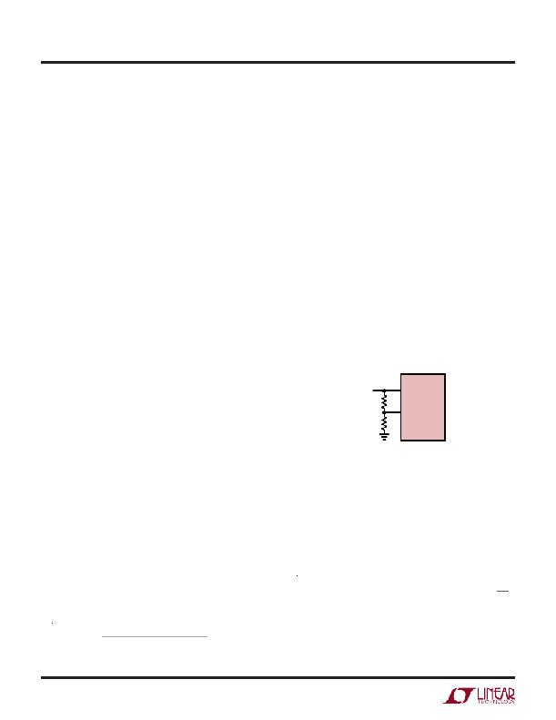
�Figure� 11� shows� how� the� maximum� output� voltage� can�
�be� set� by� an� external� resistor� divider.�
�LT3597�
�V� OUT1-3� V� OUT1-3�
�R2�
�FB1-3�
�R1�
�3597� F11�
�Figure� 11.� Programming� Maximum� V� OUT1-3�
�The� maximum� output� voltage� must� be� set� to� exceed� the�
�maximum� LED� drop� plus� 1V� by� a� margin� greater� than� 10%.�
�However,� this� margin� must� not� exceed� a� voltage� of� 10V.�
�This� ensures� proper� adaptive� loop� control.� The� equations�
�below� are� used� to� estimate� the� resistor� divider� ratio.� The�
�sum� of� the� resistors� should� be� less� than� 100k� to� avoid�
�noise� coupling� to� the� FB� pin.�
�?�
�V� OUT(MAX)� =� V� LED(MAX)� +� 1.1V� +� V� MARGIN�
�V� MARGIN� ≤� 10V�
�3597fa�
�16�
�发布紧急采购,3分钟左右您将得到回复。
相关PDF资料
LT3598IUF#PBF
IC LED DRIVR WHITE BCKLGT 24-QFN
LT3599IFE#PBF
IC LED DRVR WHITE BCKLGT 28TSSOP
LT3743EFE#PBF
IC LED DVR HP CONST CURR 28TSSOP
LT3745IUJ#TRPBF
IC LED DVR 16CH 50MA 40QFN
LT3746IUHH#TRPBF
IC LED DRIVER 32CHANNEL 56-QFN
LT3754IUH#TRPBF
IC LED DVR 16CH 50MA 32QFN
LT3755EMSE#PBF
IC LED DRVR HP CONS CURR 16-MSOP
LT3760EFE#PBF
IC LED DVR WHT/CLR BCKLT 28TSSOP
相关代理商/技术参数
LT3597EUHG#TRPBF
功能描述:IC LED DRIVER 60V TRIPLE 52-QFN RoHS:是 类别:集成电路 (IC) >> PMIC - LED 驱动器 系列:- 标准包装:6,000 系列:- 恒定电流:- 恒定电压:- 拓扑:开路漏极,PWM 输出数:4 内部驱动器:是 类型 - 主要:LED 闪烁器 类型 - 次要:- 频率:400kHz 电源电压:2.3 V ~ 5.5 V 输出电压:- 安装类型:表面贴装 封装/外壳:8-VFDFN 裸露焊盘 供应商设备封装:8-HVSON 包装:带卷 (TR) 工作温度:-40°C ~ 85°C 其它名称:935286881118PCA9553TK/02-TPCA9553TK/02-T-ND
LT3597IUHG#PBF
功能描述:IC LED DRIVER 60V TRIPLE 52-QFN RoHS:是 类别:集成电路 (IC) >> PMIC - LED 驱动器 系列:- 标准包装:6,000 系列:- 恒定电流:- 恒定电压:- 拓扑:开路漏极,PWM 输出数:4 内部驱动器:是 类型 - 主要:LED 闪烁器 类型 - 次要:- 频率:400kHz 电源电压:2.3 V ~ 5.5 V 输出电压:- 安装类型:表面贴装 封装/外壳:8-VFDFN 裸露焊盘 供应商设备封装:8-HVSON 包装:带卷 (TR) 工作温度:-40°C ~ 85°C 其它名称:935286881118PCA9553TK/02-TPCA9553TK/02-T-ND
LT3597IUHG#TRPBF
功能描述:IC LED DRIVER 60V TRIPLE 52-QFN RoHS:是 类别:集成电路 (IC) >> PMIC - LED 驱动器 系列:- 标准包装:6,000 系列:- 恒定电流:- 恒定电压:- 拓扑:开路漏极,PWM 输出数:4 内部驱动器:是 类型 - 主要:LED 闪烁器 类型 - 次要:- 频率:400kHz 电源电压:2.3 V ~ 5.5 V 输出电压:- 安装类型:表面贴装 封装/外壳:8-VFDFN 裸露焊盘 供应商设备封装:8-HVSON 包装:带卷 (TR) 工作温度:-40°C ~ 85°C 其它名称:935286881118PCA9553TK/02-TPCA9553TK/02-T-ND
LT3598
制造商:LINER 制造商全称:Linear Technology 功能描述:60V Triple Step-Down LED Driver Programmable Temperature Protection
LT3598_1
制造商:LINER 制造商全称:Linear Technology 功能描述:6-String 30mA LED Driver with 1.5% Current Matching
LT3598EFE#PBF
功能描述:IC LED DRVR WHITE BCKLGT 24TSSOP RoHS:是 类别:集成电路 (IC) >> PMIC - LED 驱动器 系列:- 标准包装:6,000 系列:- 恒定电流:- 恒定电压:- 拓扑:开路漏极,PWM 输出数:4 内部驱动器:是 类型 - 主要:LED 闪烁器 类型 - 次要:- 频率:400kHz 电源电压:2.3 V ~ 5.5 V 输出电压:- 安装类型:表面贴装 封装/外壳:8-VFDFN 裸露焊盘 供应商设备封装:8-HVSON 包装:带卷 (TR) 工作温度:-40°C ~ 85°C 其它名称:935286881118PCA9553TK/02-TPCA9553TK/02-T-ND
LT3598EFE#PBF
制造商:Linear Technology 功能描述:LED DRIVER BOOST PWM 2.5MHZ 制造商:Linear Technology 功能描述:LED DRIVER, BOOST, PWM, 2.5MHZ, TSSOP-24
LT3598EFE#TRPBF
功能描述:IC LED DRVR WHITE BCKLGT 24TSSOP RoHS:是 类别:集成电路 (IC) >> PMIC - LED 驱动器 系列:- 标准包装:6,000 系列:- 恒定电流:- 恒定电压:- 拓扑:开路漏极,PWM 输出数:4 内部驱动器:是 类型 - 主要:LED 闪烁器 类型 - 次要:- 频率:400kHz 电源电压:2.3 V ~ 5.5 V 输出电压:- 安装类型:表面贴装 封装/外壳:8-VFDFN 裸露焊盘 供应商设备封装:8-HVSON 包装:带卷 (TR) 工作温度:-40°C ~ 85°C 其它名称:935286881118PCA9553TK/02-TPCA9553TK/02-T-ND